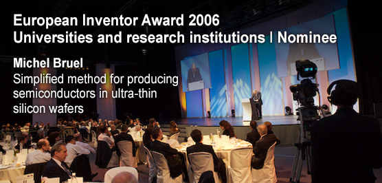
Michel Bruel
Semiconductor wafer
An Insulating Layer Leads to Semiconductor Success
In 1993, Dr. Michel Bruel patented a process for the production of thin, semiconductor material films while working as a researcher at Commissariat a l’Energie Atomique-Leti, one of Europe’s largest microelectronics research institutes, in Grenoble. Bruel’s invention, known as the Smart Cut process, was the pioneering step towards large-scale production of high-quality silicon-on-insulator (SOI) wafers at a reduced cost. SOI wafer production methods previously existed but weren’t used extensively, owing to their expense and technical unreliability.
Bruel’s invention developed a single-step, cost-effective process for adding an ultra-thin layer of insulation to dinner-plate size silicon wafers, onto which microchip circuits are etched. The layer of insulating material, such as silicon oxide or glass, prevents electricity from leaking into the silicon, letting chips run up to 40 percent faster while using half as much power. As the chips require less power, they also produce less heat, of vital importance in large servers, where heat removal can be a problem.
SOI produces higher-performing, lower power devices than traditional bulk silicon techniques. Circuits manufactured on SOI material go on working even under the most critical conditions, notably radiation and extreme temperatures, as the insulating layer protects the circuit from interference.
Two CEA-Leti researchers, Andre-Jacques Auberton-Herve and Jean-Michel Lamure realised the potential of the technology and set up a start-up, called Soitec, in Brenin, near Grenoble. The researchers were convinced that one day SOI would become a standard material for mass-market components, essential to mobile phones, gaming consoles, automotive power sensors and innumerable other portable devices. Bruel, meanwhile, continued his SOI commercialization efforts as head of the integration and assembly laboratory in CEA-Leti’s microtechnologies department.
Soitec spent years after the company’s 1992 launch struggling to make the technique commercially viable. Their breakthrough came when Philips became the first company to use SOI-based components in an audio amplifier. Now the world has finally caught up with Soitec. The company has become an example of a successful move from fundamental research in the heart of a laboratory dedicated to nanotechnologies to worldwide industrial leadership in an innovative and competitive domain. Of course, Bruel’s technology lies at the origin of Soitec’s success.
Soitec now supplies 80 percent of the SOI wafers used by chipmakers around the world, while licensees provide an additional 10 percent. Thanks to landmark deals with giants such as IBM, Philips, and Advanced Micro Devices, Soitec’s 2005 sales were expected to top 135 million euros, a threefold increase from four years ago. The company now employs 530 people, up 100 percent since 2000.
Freescale Semconductor supplies Apple Computer with Soitec-based chips for laptops. And both the Sony Playstation 3 and the next-generation Microsoft Xbox use chips built on Soitec wafers.
The company has recently signed a contract with AMD that will bring in 126 million euros during 2006. Soitec plans this year to start two additional 300mm wafer production lines, with another eight lines planned for the next financial year.
The higher speed and lower power afforded by SOI chips have already proven the technology’s benefits in high-performance markets. In future, SOI has the potential to provide significant opportunities in lower power. “SOI will gradually replace silicon as the basic material in microelectronics. There is no going back now,” said Lamure.
Contact
European Inventor Award and Young Inventors Prize queries:
european-inventor@epo.org Subscribe to the European Inventor Award newsletterMedia-related queries:
Contact our Press team#InventorAward #YoungInventors


